From densification of packages to the miniaturization of semiconductors, Nippon Micrometal invests heavily in R&D to ensure its bonding wires can cater to the latest industry needs.

In the last 25-30 years, Japan has seen the rise of regional manufacturing competitors who have replicated Japanese monozukuri processes but at a much cheaper labor cost, pushing Japan out of mass industrial markets. Yet, we still see many Japanese firms as leaders in niche B2B fields such as materials and machinery for semiconductor production. How have Japanese firms been able to maintain their leadership despite stiff price competition?
Looking back at history, Japan has lost in terms of mass production, but research and development-wise, Japan still maintains its strength. One of the reasons Japan is lagging behind in terms of mass production is, of course, this price competition you mentioned. At the same time, we see slow decision-making has become quite the hindrance and reflecting back on these factors, our company has established a system where we can readily answer to mass production. We have our own research and development facility, and our own methodology and intensive knowledge derived from our own experiences at Nippon Steel, our parent company.
Another key strength of our company is the securing of patents, and this is very crucial in terms of our global expansion strategy. We have been able to secure patents across the globe, and we are licensing our technology to our competitors.
Japan is the oldest society in the world and has a rapidly shrinking population. Two major challenges stem from that: the first being a labor crisis, meaning a smaller pool of talented young graduates coming in to replace older workers. The second is a shrinking domestic market. Can you tell us what are some of the challenges and opportunities this demographic shift is presenting for Nippon Micrometal?
As you say, the demographic issue is posing a significant threat to Japanese companies as a whole and what we are trying to do here at Nippon Micrometal is to fortify our R&D team and maintain that domestically. Nurturing human resources is very important, and at the same time, we are focusing on automation in order to use less manpower for production and that applies not only domestically, but overseas as well. We are looking to produce products in a more automated manner. Regarding the shrinking domestic market, we actually do not consider that a threat since a majority of our customers are overseas. These customers are the major semiconductor players globally, so what we are doing is actually finding an appropriate partner in each locality so we can collaborate and tackle the semiconductor market, which actually only has one big market globally.
Predictions in 2020 had the global semiconductor market growing to be worth USD 1 trillion by the year 2030. Obviously, a great many things have happened since then: the COVID-19 pandemic, as well as the worldwide chip shortage. This has led to many regional leaders pushing to expand their domestic production. What opportunities do these regional pushes present for your firm?
Currently, the production of semiconductors is focused in Taiwan and China, but by diversifying, we are creating a very advantageous situation in terms of our business continuity plan. We find no negativity in the expansion of local production and hope to find more opportunities for ourselves to grow. In China and Taiwan, there are some geopolitical concerns, so by diversifying, we are making production more sound and secure.
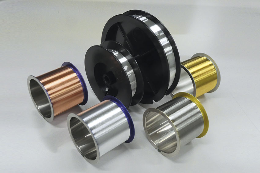
Nippon Micrometal makes bonding wires for semiconductor packages. Gold can be very expensive and a cheaper alternative to this is copper, however, it also oxidizes, meaning that users need to be very wary when it comes to bonding processes or storage. Your Advanced Copper Wire EX resolves this issue and can be used in advanced packages. How were you able to overcome this oxidation challenge for your Advanced Copper Wire EX?
I was a leader of the EX wire development and managed each phase of it and copper wire, as you know, always has had this issue with oxidation. We overcame this by selecting palladium as a coating material and controlling the palladium metal coating at a nano level. We developed our unique plating and drawing technologies and with them, we were able to succeed in mass-producing Palladium Coated Copper (PCC) wire. Gold has been used for 50 years now, but with prices surging, replacing gold wire with PCC wire that is robust against oxidation has been very effective and enabled our customers to reduce their costs significantly.
Can you tell us more about your LF35 Micro Solder Ball and how this product is superior to conventional micro solder balls?
We started developing the LF35 when mobile phones became popular, and it provides an excellent drop performance of surface mount electronic components. What we have invented is a very unique composition of metal based on our own methodology. It has high reliability and connectivity.
When it comes to semiconductors, we are seeing the utilization of new materials such as silicon carbide and gallium nitride. How are you adapting your wires to these new materials?
Currently, our copper and gold wire products are focused on silicon-based semiconductors which are used for a more high-density type of semiconductor. On the other hand, in the area of power semiconductors, we are anticipating a switch to new technologies, such as silicon carbide (SiC) technology. For example, with the transition to EVs, SiC technology will be essential for a transition from a 400-volt to an 800-volt battery charging system. We are focused on developing new types of wires for power semiconductors and also conducting research into advanced copper wires as copper has much higher electrical conductivity than aluminum.
Could you tell us a little bit more about your R&D strategy and are there any specific products that you are currently working on that you would like to showcase?
We have a few products that will be released in the fall of 2022 and they focus on upgraded versions of our wires with newly added functionality. Our R&D focus currently is on the bonding wires for automotive applications that require high reliability under high temperature operation. Our advanced PCC wire as well as bare copper wire and silver alloyed wire are applicable to new types of technology. We are looking to add further functionality too, but unfortunately we cannot disclose further information as the patents are still pending.
Miniaturization has been linked to the history of electronics, with Moore’s Law stating that the number of transistors on a microchip doubles every two years. Right now, we are seeing a huge trend when it comes to this idea of miniaturization, as products are becoming smaller, yet have more functionality than ever. How is Nippon Micrometal reacting to this miniaturization trend?
Miniaturization is having an impact on our products and we need to continuously improve our products to cater to the higher densification of semiconductor packages. We see that not only are they getting smaller, but we also see a move towards more stacking of die in 3D semiconductor packaging. With this regard, we must make the diameter of the wire smaller and keep improving our wire technology. It is vital that we keep ourselves updated with all the advancements in the semiconductor field.
When the transistor was first invented, there was only a single wire on a surface. But, now with high densification and die stacking, we see a semiconductor package with more than 1500 pins, and that in turn requires more than 1500 wires. It is extremely difficult to keep those wires from touching each other and causing a short circuit. Wires are now down to the size of 16 microns and even smaller, which would be less than one-fourth the thickness of a human hair, and current wire bonding technology makes more than ten wire bonds in one second, so as you can probably understand, this is a very complex procedure.
You mentioned that the majority of your customers are overseas, so I am curious to know how you managed to achieve this. Why do overseas firms choose Nippon Micrometal for their bonding wires?
Our strength can be described in three aspects, and the first is the quality itself. Our customers use our wires as the last step in their semiconductor productions, so if the wire bonding were to fail, the whole process must be discarded and would be considered a waste. With that in mind, you can understand why reliability and high quality are essential to our business.
Secondly, we provide aftercare to customers and should any issues arise when using our products, we are ready and willing to provide solutions for customers. Technological support is one very strong advantage that we provide. Lastly, we conduct R&D in advance and consider potential future trends. With our cutting edge technology, we develop our products tailored to individual companies’ needs.
Are there any trends that you have identified that could occur in the future?
High-density integration is an upcoming trend in semiconductors. Also, 30% of semiconductor packages still use gold wires, so replacing those with silver or copper is our main focus currently. The next generation of vehicles is coming with the emergence of the CASE era, with autonomous driving becoming a very real future. Reliability in that field is crucial and we also have our eye on the advancements in this field.
In 2000, you opened your first international operation in Malaysia, and since then, you have expanded into the Philippines and China. What other countries or regions have you identified for further expansion, and what strategies will you employ to do so?
We would like to continue to expand overseas, and ultimately establish a base in each locality that we operate in, however, we still want to retain our R&D in Japan. Through our R&D center in Japan, we collaborate with many overseas companies and looking forward, we would like to continue with these collaborations.
Imagine that we come back in five years' time and have this interview all over again. What would you like to tell us and what are your dreams and goals for Nippon Micrometal?
We are currently developing a plan for 2030 and we want to realize our objectives one by one. Overall, my goal is to make this company a globally recognized company all across the world.


0 COMMENTS