We spoke to Terushi Shimizu, Representative Director, President & CEO of Sony Semiconductor Solutions Corp, to learn more about the company’s image sensor technology and its applications, which include smartphone cameras, automotive, DX and edge computing.

The Japanese monozukuri philosophy is closely related to the kaizen approach, which emphasizes constant improvement in all aspects of production. “Sense the Wonder” is the Sony Semiconductor Solutions (SSS) Group slogan, with this in mind, what is SSS’s unique interpretation of monozukuri?
In monozukuri, the important question is where to place the company’s core competencies. Our core competences in monozukuri lie in its world-class advanced technology and its ability to integrate these technological capabilities with a series of processes from design, development, and manufacturing at a high level. All these competencies are supported by our advanced manufacturing technology and quality control system.
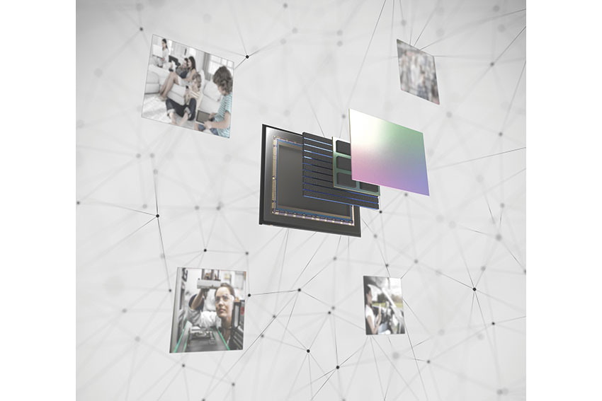
In particular, our CMOS (Complementary Metal-Oxide-Semiconductor) image sensor is an analog device in which the ability to integrate becomes extremely important in order to realize characteristics such as sensitivity and minimal noise. This is an area where SSS can differentiate ourselves from competitors. By vertically integrating our processes of design, development and manufacturing in-house, we are able to create products with high technological capabilities and in turn, sustainably elevate customer values. Although, comparatively, if it were a digital device with which integration of those processes would not be as important as in analog, we might not have been able to maintain our current superior position.
We believe that the functional values which we provide on our image sensors have added value that far exceeds the cost competitiveness that Asian companies emphasize. For example, in the automotive field where the required level of standard is very strict, we have been implementing thorough quality control to contribute to assuring safety and security, as a result, SSS has outperformed its competitors in terms of temperature resistance and failure rate.
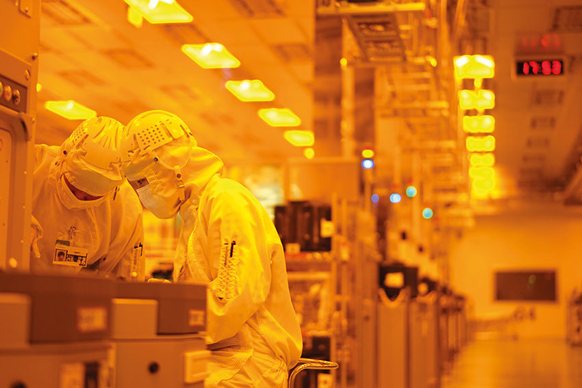
Clean room at Nagasaki Technology Center
Back in the 1980s we saw that demand for semiconductor products, especially for DRAM, was met predominantly by Japanese companies like Toshiba, Fujitsu and Hitachi who held dominant market shares. In the 2000s however, their market share sharply declined, yet today, Japan still dominates when it comes to semiconductor functional chemicals & machinery. What is your assessment of the current Japanese semiconductor industry, and what is the unique contribution that Japanese firms bring to the semiconductor market?
Because image sensors are analog devices, they do not require state-of-the-art facilities. We are able to differentiate by our know-how in design, development and manufacturing which had been accumulated through years of CCD (Charge Coupled Devices) image sensor development. On the other hand, the digital semiconductor businesses, such as DRAM, logic LSI, and memory, require huge capital investment in advanced processes for manufacturing to achieve miniaturization and maintain product competitiveness.
SSS decided to concentrate its resources on the image sensor business in the late 2000s as a business that relatively does not require huge process development costs and capital investment burdens on a regular basis, as such it succeeded in enhancing its competitiveness and securing its market position. The principal products of our image sensor business are highly customized and differentiated. As a result, our business model is somewhat less vulnerable to volatility from the so-called “Silicon Cycle”. Our sales volatility is further reduced through differentiation in our customer base and high market share achieved over the last couple of years.
In addition, as we combine image sensors and AI to a wide variety of applications, such as IoT, driving automation, games & immersive entertainment, and advanced medical technology, we expect further product and customer diversification to enhance the stability of the business.
Prior to the outbreak of the COVID-19 pandemic, industry experts were predicting that the semiconductor market would grow to $1 trillion by 2030. However, with the COVID-19 pandemic, we have seen chip shortages worldwide and regional leaders pushing to expand domestic production capacity so as to not rely solely on pure-play foundries. SSS has partnered with TSMC to build a new foundry in Kumamoto, what opportunity will this new domestic capability together with these new regional pushes present for SSS?
90% of our CMOS image sensor business uses stacked technology – pixels stacked on top of logic wafers – and we use an external foundry to get the logic wafers as internally, we have only very small production capacity. In order to increase the foundry capacity for our logic wafers we partnered with TSMC. As the global semiconductor demand is expected to continue to grow, we expect that the new TSMC fab, “Japan Advanced Semiconductor Manufacturing (JASM)”, will contribute to the stable supply of logic wafers not just for SSS, but also for the overall industry.
Also, from the perspective of the Japanese semiconductor industry as a whole, if the establishment of JASM stimulates the activities of partner and service companies that support its production activities, it might lead to the revitalization of the industry which we highly welcome. We would like to support JASM so that it can take root in the local community and get its operations on track at an early stage.
By revitalizing the semiconductor industry, we hope that the younger generation will have an interest in this industry, and furthermore broaden the base of human resources aspiring to enter this industry.
Traditionally in the Japanese semiconductor industry, there has not been that much collaboration between companies in developing products, but in recent years, SSS has partnered with TSMC and Denso in this respect. What role does co-creation play in your product development? Are you looking for such partnerships internationally?
“To spark imaginations and enrich society through the power of technology” — this is SSS's company mission. Toward this mission, we spare no effort in increasing our corporate value, and enhancing our technology and manufacturing capabilities. To this end, we will work on what needs to be pursued as an individual company, and if we can achieve our mission better by working with partners, we will choose co-creation with partner companies. From our point of view, there is no difference between partnering with another Japanese company and us partnering with a foreign one. The most important point is that the relationship is one that is built on a solid foundation of trust and is not just a front for formality’s sake.
In 2015, when SSS was seeking to strengthen its domain in the field of sensing technology, it acquired Softkinetic, a small Belgian company that at the time was in a leading position in distance measurement technology. The two companies, which shared a common motivation to “bring superior sensors for depth/distance measurement to the world,” formed a strong partnership based on trust and confidence and have been seeing some good results as the SSS group to this day while leveraging on each other’s strengths. If the connection is superficial and without trust, it won’t work.
SSS commercialized the world’s first image sensor with AI functionality in 2020. How does integrating cutting edge AI, such as deep neural network processing, into Intelligent Vision Sensors add value to your image sensing technology?
We started the development of an image sensor with neural networks – the AI engine – on top of it in 2016. Around that period, we were questioning how we could add more value to our image sensor technology, and we thought it would probably be a “solutions business”. Looking outside, the demand for cloud business typically handled by companies, such as GAFA (Google, Apple, Facebook, Amazon), continues to grow as new IoT devices continually get connected to the internet. Based on this situation, we assumed that those companies, as well as society, will sooner or later face various issues if it continually relies too much on cloud computing. That situation would result in a huge operational cost burden, and from an environmental point of view, raising all information to the cloud would require huge levels of power consumption and there would also be privacy issues. If we could harness AI processing on edge to perform some of the same functions as cloud computing, it would probably contribute to resolving those issues, so this is why we’ve decided to add a tiny AI engine to the image sensor.
The concept of our intelligent vision sensor is to output only the necessary information as metadata depending on the application. To have the sensors used in as many applications as possible, we focused on their small size, low power consumption, and speed. This was something that was not yet available in the world, and the engineers had to question themselves over and over on how it would be used, how much processing should be done on the edge, and what AI engine is necessary for that purpose – these were the most difficult questions for them – so they gathered the wisdom and technical capabilities within SSS group to come up with the world’s first image sensor with AI processing capability.
Our intelligent vision sensor “IMX500” is a key device that will lead to the development of optimal systems in which the edge and the cloud function in synergy. It will support our partners in popularizing and expanding environmentally conscious sensing solutions using edge AI and deliver new value and help solve challenges faced by various industries.

Intelligent Vision Sensor IMX500
What applications do you see for this technology, and what kind of clients will benefit the most from it?
We imagine a huge market and variety of applications. In 2019, we visited Microsoft’s office in Seattle to present our concept of IMX500. They had been concerned about the future in terms of managing the ever-increasing number of edge devices only with cloud technology, so Microsoft engineers were very impressed by IMX500 and expected that it would contribute in realizing the synergy of the edge and the cloud. Thus, we started to work together to simplify access to computer vision solutions with efficient allocation of resources between the edge and the cloud. Through the synergy of the edge and the cloud, six challenges are sought to be resolved: control of data volume, addressing privacy concerns, reduction of electric power consumption, improvement of latency, service continuity and strengthening security. The IMX500 will play an important role as a key device to that end.
There are probably a lot of potential applications for it. A smart city trial in Rome is underway using the IMX500 to solve social issues like traffic congestion and accidents. It also plays a role in a solution developed by U.S. company Nomad Go to reduce power consumption by making air conditioning systems in buildings more intelligent. Many other PoCs (Proof of Concept), including smart retail and smart manufacturing, are in progress.
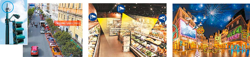
IMX500 targeting various applications
Can you explain to us more about your current R&D strategy? What are some of the key things that you're working on that you could share with our international readership?
In addition to “imaging” technology, which is used to take beautiful pictures, our image sensors have been bringing various solutions to “sensing” areas by acquiring and utilizing information which cannot be seen by the human eye. In imaging for mobile applications, based on the technological development we have underway, we believe to find imaging technologies evolving on the axes of still images, videos, and production. To provide people with new imaging experiences, we must continue to enhance our hardware to realize performances like super high dynamic range (HDR) and zoom functions for still images, high image quality and high-speed reading at 8K for video, and production functionality, like how to take a good picture.
As for the sensing area, we expect a “Sensing Society” is imminent and in such a society, sensing technology will become an important foundation. Sensing is a key element in the development of IoT and DX in all fields such as mobile, automotive, industry, and VR/AR applications such as the Metaverse, which has become trendy these days. Image sensors can gather a considerable amount of information which makes us believe that their potential and contribution can be particularly profound. Toward an enriched sensing society backed by safety, security and high efficiency, we will continue to pursue image sensor technology.
To give an example, we commercialized a Short-Wavelength InfraRed (SWIR) image sensor in 2020, which uses a range of infrared spectrum outside the visible light band and allows users to distinguish various things that may look the same to the naked eye but are in reality different. Using SWIR sensors, users can identify things like colorless oil and water, sugar and salt, and even check the contents through the plastic container. It also allows for the recognition of objects 50km away clearly through smoke and haze. A principal application of this sensor could be to highlight contamination at the production line or sorting materials at recycling sites with enhanced accuracy compared to human eyes, so this device can also make a contribution to safety and the environment.
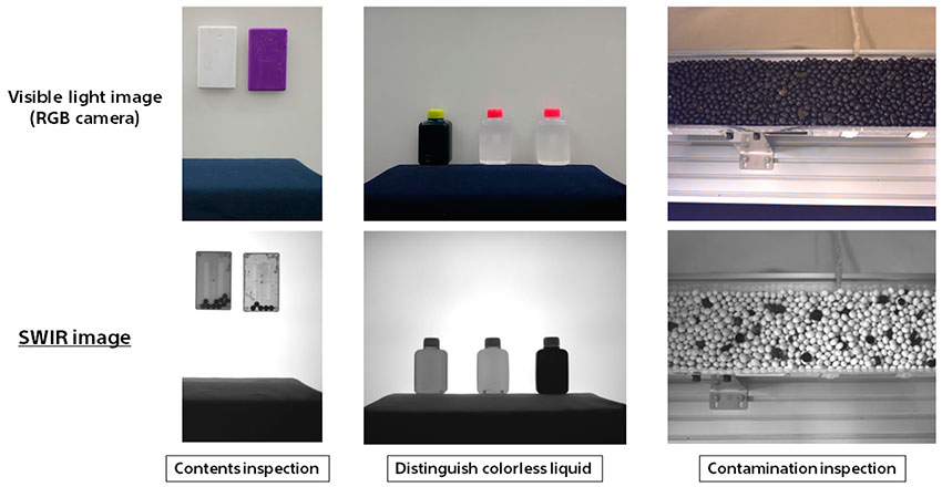
Comparison of images taken with (Upper) RGB camera and (Bottom) SWIR image sensor
One of the biggest customers for your sensors is the automotive field, which increasingly requires image sensors to identify objects in the surrounding environment. The sensors you supply to the automotive industry must be able to work across a wide variety of environments and climates where temperature variations are extreme. Can you explain in more detail some of the solutions or technologies you have developed for this field?
Image sensors that accurately acquire information from inside and outside the vehicle are becoming increasingly important as Autonomous Driving (AD) technologies evolve. Our imaging and sensing technologies will contribute to ADAS (Advanced Driver Assistance Systems) and to the safety and security of future AD. We started the automotive image sensor business around 2012, when we saw the progress in the development of automatic braking and the demand for automotive cameras grew. We have gradually gained trust from our partner companies by continuing to produce innovative products that meet and sometimes overwhelm their needs while satisfying automotive quality. Through the acknowledgement from car manufacturers and suppliers on our performance level, our sensors are now being installed in their completed vehicles.
The major factor behind realizing such a level in this automotive field, is the solid foundation of our proprietary technology for high image quality which we had cultivated in consumer camera and smartphone applications. In addition to high sensitivity and high resolution, we have been advancing the development of solutions unique to automotive use: weather resistance, noise suppression even in low illuminance and high temperature environments, and technology for capturing LED lamps in a wide range of illuminance scenes. Taking temperature, for example, competitors’ products sometimes fail in image quality at high temperatures, whereas our products can output stable images even at 125 degrees. In addition to image sensors, we have also just shipped the SPAD depth sensor for automotive LiDAR applications, a sensing solution that can accurately detect and recognize road conditions as well as the position and shape of vehicles and pedestrians.
Through our inquisitive spirit and passion for pursuing a higher degree of technical perfection that are rooted within the Sony Group since its foundation, we are able to bring about products which contribute to safety and security when it comes to mobility.

360-degree sensing and detecting around a vehicle
SSS spun off from the Sony Group and started its business as a subsidiary company in 2016. Can you tell us why this structural change happened and how SSS benefited from it, especially when it comes to your international operations?
The Sony Group has shifted to the current architecture with the aim of each business entity becoming more independent and autonomous and contributing to improving the corporate value of the entire Sony Group. We, SSS, started our business in April 2016. In every aspect and day by day, we are working on the evolution of technology and the improvement of corporate values. To that end, we must enhance our presence in society and evoke a favorable response from various stakeholders as well as the large number of partner companies. This is extremely important for talented personnel all over the world to choose our company. In order to clearly convey our company’s message, we came up with the corporate slogan “Sense the Wonder”. It is a verbal form of what the SSS Group will continue to value in the future.
We have bases with various functions overseas. As we expand our business and the areas of challenge, I do not deny the possibility of further expanding our overseas bases, if necessary. To that end, it is indispensable that our company can sustainably attract highly motivated personnel who sympathize with the SSS philosophy.
Imagine we come back to interview you again in three years' time for your company’s 10th anniversary. What would you like to tell us, what are your goals and dreams for the company and what would you like to have achieved by then?
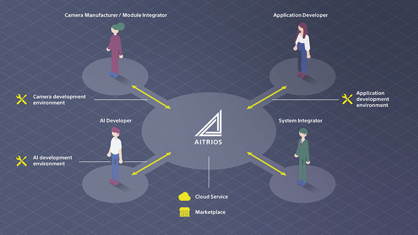
At this point, we have set an internal goal for 2030 and are moving forward towards it eight years from now. It’s difficult to see beyond that, but I think it is essential not only to evolve hardware, but also software and the solutions business in order to increase our corporate value. SSS have released a number of image sensors for sensing applications to the world, but we’ve not reached our goal until we find our partners utilizing these sensors to implement more solutions in society. “AITRIOS”, launched last year, is an edge AI sensing platform that makes it easy for solution providers to build solutions using our image sensors specialized in sensing applications. If AITRIOS advances the social implementation of sensing solutions, our hardware will become more indispensable and not lose its value. Based on this assumption, I’m hoping that over the next 10-20 years, the scale of solutions business ratio will become bigger than the hardware business ratio. In the next 30-40 years I believe it certainly will.


0 COMMENTS